|
||||||
|
\главная\р.л. конструкции\трансиверы\цифровая шкала с цапч\... |
![]() Перевести
эту страницу на русский язык
Перевести
эту страницу на русский язык
DIGITAL DISPLAY FOR THE KW-2000B TRANSCEIVER
AN UPDATE FOR A FINE OLD RIG PETER
J. COOK, G4NCA
IN the face of ever-increasing transceiver prices, the prospect of upgrading older equipment becomes increasingly attractive. A popular example of such a piece of equipment is the KW-2000B, offering 5-band coverage, SSB/CW, with an input power of 180 watts p.e.p., usually available at a fraction of the price of its present day counterparts. A comparatively simple transceiver such as the '2000B lends itself to modification (for example, see "Modifying the KW-2000A Transceiver for the 10 MHz", Short Wave Magazine, May 1982).
One feature the author has found very annoying with the rig is the inaccuracy of the analogue dial, it being very diffficult to net precisely on any specific frequency. The addition of a digital readout would enable an accurate check on frequency (and also show just how much the VFO drifts during operation . . .), allowing very accurate netting.
A study, of the various mixing processes carried out in the KW reveals that the VFO tunes from 2.5-2.7 MHz, producing a 200 kHz allocation for each master oscillator crystal. The output from the VFO is mixed with 455 kHz SSB to produce a variable IF of 2.955-3.155 MHz. This signal is subtractively mixed with a crystal master oscillator to produce RF in the appropriate amateur band. A consequence of this mixing process is that as the transceiver is tuning to a higher frequency, the VFO frequency is in fact decreasing. Hence any digital readout must read '200 kHz' when the VFO is at 2.5 MHz, falling to '0 kHz' when a frequency of 2.7 MHz is attained.
Operation
The basic operation of the display is probably best described with the aid of
Fig. 1, a simplified block diagram. All clock pulses are derived from a 2.7 MHz crystal
oscillator, applied to input A, the sinewave output from the VFO being squared off and applied to input
B.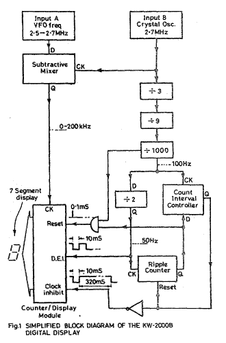 These two signals pass to the clock and data
inputs, respectively, of a D-type bistable, forming a digital subtractive
mixer. When the VFO is tuned to 2.5 MHz, a frequency of 200 kHz is produced at the Q
output, falling to 0 kHz as the VFO frequency rises to 2.7 MHz, in accordance with the requirement illustrated in the previous
paragraph. Additionally, the 2.7 MHz signal undergoes a division of 27,000 to generate 100 Hz clock for timing
purposes. A further division by 2 is implemented to generate 50 Hz pulses, connected to the display enable input
(DEI) of the counter/display module. Whenever this input goes high, the data stored in the counters is applied to the 4-digit, 7-segment,
display; hence in this application the display will be on for lOmS, followed by a lOmS
off, or blanking period. It is during this period that counting must occur
(otherwise the display will be a meaningless jumble of figures), and this is achieved by allowing the clock inhibit pin of the
counter/display module to go low during an appropriate period of blanking. The interval between counting periods is determined by the action of the ripple
counter, in conjunction with the count interval controller (another D-type
bistable).
These two signals pass to the clock and data
inputs, respectively, of a D-type bistable, forming a digital subtractive
mixer. When the VFO is tuned to 2.5 MHz, a frequency of 200 kHz is produced at the Q
output, falling to 0 kHz as the VFO frequency rises to 2.7 MHz, in accordance with the requirement illustrated in the previous
paragraph. Additionally, the 2.7 MHz signal undergoes a division of 27,000 to generate 100 Hz clock for timing
purposes. A further division by 2 is implemented to generate 50 Hz pulses, connected to the display enable input
(DEI) of the counter/display module. Whenever this input goes high, the data stored in the counters is applied to the 4-digit, 7-segment,
display; hence in this application the display will be on for lOmS, followed by a lOmS
off, or blanking period. It is during this period that counting must occur
(otherwise the display will be a meaningless jumble of figures), and this is achieved by allowing the clock inhibit pin of the
counter/display module to go low during an appropriate period of blanking. The interval between counting periods is determined by the action of the ripple
counter, in conjunction with the count interval controller (another D-type
bistable).
Assume that the ripple counter has just been reset to гего. It will count up in binary upon receiving 50 Hz clock pulses from the divider chain. For the time interval that the output Q4 is low, the data input of the count interval controller will be held low, as will the Q output irrespective of 100 Hz. clock pulses being applied to the clock input. However, once 23 clock pulses have been received, Q4 goes high. When the next clock pulse is applied to the controller, Q goes high, causing the clock inhibit input to go low, allowing lOmS-worth of pulses from the subtractive mixer to reach the counters. At the same time, the ripple counter is reset to zero, causing Q4 to go low. On receiving its next clock pulse, the Q of the controller goes low, and so the process continues. ... It will also been noted that as Q4 goes high it opens the way for a O.lmS reset pulse immediately proceeding a count period, resetting the count to zero.
This control logic at first may seem unnecessary as it would appear much easier to count during all blanking periods. This method was originally adopted by the author, but an intolerable amount of jitter occurred due to the 100 Hz (least significant) digit changing alternately between two digits, this change taking place at any frequency from 0 to 50 Hz.
With the circuit as shown (Fig. 2), the count rate is one count every 320mS, which is the best compromise between annoying jitter and sluggish tracking of the
VFO during tuning. For a faster count rate of 160mS, the data input of the controller should be connected to Q3 of the ripple counter, a 640mS rate is available by connection to Q5, etc., etc. . . .
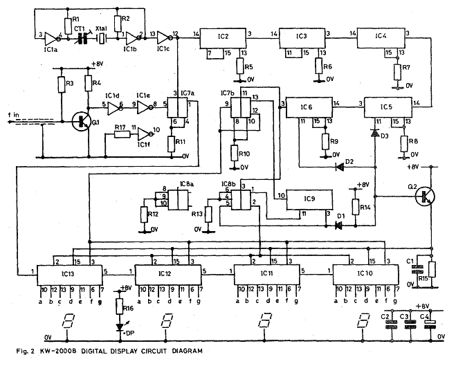
The 2.7 MHz crystal and associated inverters present fast squarewaves to the divider
chain, comprising of IC2 (divide by 3), IC3 (divide by 9), followed by IC4,5,6— all decade
dividers. The resultant 100 Hz squarewave undergoes a further stage of division by 2, IC7& thereby supplying display enable pulses to the
counter/display module, IC10, 11, 12, 13. IC7a forms the subtractive mixer, being fed with 2.7 MHz clock pulses and a squarewave representation of the VFO frequency
(produced by Ql and two associated inverters), the mixer output being applied to the input of the
counter/display module. The ripple counter, IC9, is fed with 50 Hz clock pulses and is controlled by 1С8Й, the count interval
controller, applying clock inhibit pulses to the counter/display module. Dl-4, Q2 and associated circuitry forms a 3-input AND gate and is used to control reset pulses to the
counters. It will be seen that a positive potential (supplied via R14), will only be present when all of the diodes are reverse
biased, i.e. when pin 11 IC6, pin 11 IC5, pin3IC5, are all high. This will only occur during the O.lmS period before any count
period. During this period, Q2 conducts and a high pulse resets the counters.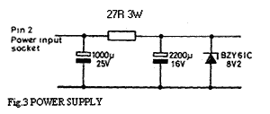
Fig. 3 shows a suitable power supply for the display, power being drawn from the + 12V DC available within the rig, used for relay switching.
Modifications
See photographs. The prototype unit was constructed on
Veroboard (using 1С sockets and usual CMOS precautions), and mounted in a small aluminium box 100 x 100 x 30mm. in
dimensions, in turn mounted on three, 50mm. standoffs above the Tx/Rx
relays. 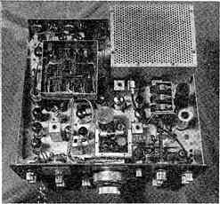 The original analogue dial was removed and a 4-digit, 7-segment, LED display mounted on
Veroboard and slotted in front of the VFO box was added. To create a more
'professional' look, the perspex window was removed and a grey border (surrounding the
display) was added using aerosol spray paint.
The original analogue dial was removed and a 4-digit, 7-segment, LED display mounted on
Veroboard and slotted in front of the VFO box was added. To create a more
'professional' look, the perspex window was removed and a grey border (surrounding the
display) was added using aerosol spray paint.
Above, general layout of G4NCA's
prototype. Below, details of inside the VFO box showing the addition of Cx.
(In the prototype, as a 47pF capacitor was not to hand, a 56pF was connected in series with a 470pF).
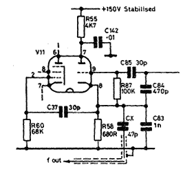 Fig. 4 details how RF pickup from the VFO was
derived. Initially RF pickup was achieved from the buffered output from the VFO
box; this arrangement worked fine on receive, but a 'scope placed at this point during transmit revealed a multitude of frequencies due to the action of close-coupling with the balanced
mixer, V4. The addition of Cx (47pF silver mica) into the VFO proved to have not detrimental
effects. Removal of the top of the VFO reveals a convenient free tag on which to mount
Cx, and a small hole drilled in the side of the VFO box is used to pass the miniature
co-ax. Bostik, or a similar adhesive, is used to secure the capacitor and other wiring from the effects of
vibration.
Fig. 4 details how RF pickup from the VFO was
derived. Initially RF pickup was achieved from the buffered output from the VFO
box; this arrangement worked fine on receive, but a 'scope placed at this point during transmit revealed a multitude of frequencies due to the action of close-coupling with the balanced
mixer, V4. The addition of Cx (47pF silver mica) into the VFO proved to have not detrimental
effects. Removal of the top of the VFO reveals a convenient free tag on which to mount
Cx, and a small hole drilled in the side of the VFO box is used to pass the miniature
co-ax. Bostik, or a similar adhesive, is used to secure the capacitor and other wiring from the effects of
vibration.
Conclusion
The display has been in use at the author's QTH for several months, proving to be invaluable for netting and providing a very economical solution to the problem (the prototype was constructed for less than £15 inclusive). The use of a screened housing eliminated all the usual 'nasties', none being detected whilst mnning the rig into a dummy load.
DIGITALISATION OF THE KW-2000B TRANSCEIVER, PHASE II
A SIMPLE ADD-ON VFO STABILISER TO COMPLEMENT THE DIGITAL DISPLAY DESCRIBED IN LAST MONTH'S ISSUE PETER J. COOK, G4NCA
ONE of the fascinating aspects of modernising older equipment (or for that matter, prototype construction) is that no sooner has a problem been identified, solutions found and modifications completed, than attention is brought (as a result of the initial modification) to other, often more subtle, shortcomings within the equipment. A consequence of this is that a continuous process is set up of successive modifications, with (hopefully) an end product that performs exactly to the individual's wishes. This approach is undoubtedly the best for home construction, ensuring that individual circuit elements do in fact work before stringing them all together. There is nothing more frustrating, having neatly built a large project, than turning on to find nothing happens (and even worse, seeing it go up in smoke!), to be faced with the prospect of breaking it down to fault-find. It was for this reason that the above title was chosen, this unit being the second modification undertaken on the 'old faithful' KW-2000B.
Having constructed a digital frequency display for the KW-2000B, it rapidly became apparent just how much the VFO drifts from initial turn-on, and indeed for several hours after. When using the rig for CW or SSB contacts this drift is quite tolerable, simply necessitating a slight tweak of the tuning every now and again. However for the more frequency 'sensitive' modes such as RTTY or SSTV the problem becomes more acute; for instance, in the author's case, obtaining reliable copy from the Sunday morning GB2ATG RTTY broadcasts on 80m. would involve tracking the VFO throughout the transmission. Additionally, this inherent drift proves to be very annoying for the distant receive station during transmission, in turn having to track his/her VFO, often resulting in the QSO wandering up and down the band at an alarming rate.
As much of the work in producing some type of digital stablisation unit had already been undertaken with the construction of the digital display, a simple add-on unit became a very attractive solution to the problem.
Within the VFO tank circuit of the '2000B there are (very conveniently) two DC controlled varicap diode branches; one of which is used in the IRT circuitry, the other involved in the calibration adjustment of the now obsolescent analogue dial. Use is made of this in the stabliser circuitry, enabling any offset frequency to compensate for drift to be created by a small change in the steady reverse bias DC voltage across the varicap diode. An increase in this voltage will reduce the capacitive effect of the diode and cause the frequency to rise. Correspondingly, a reduction in voltage will increase the capacitive effect and the frequency will fall.
Operation
The basic outline of the system is shown in Fig. 1, all power, control and timing signals being derived from the digital display board. Input pulses, supplied by the subtractive mixer (IC7) in the display board are applied to the clock input of the BCD counter, IC14. The signal applied to the clock enable input of the counter is, in fact, exactly that applied to the counters in the display board.
Tables of Values
Fig. 2
R18 to R21, R23 to R25 = 47K, R22 = 1M, R26, R27 = 1K, R28 = 470K, C5 = 100 pF C6 = 1000
pF C7 = 220 mF 12V dec. C8 = 100 nF polyester
Note: capacitors C5, C6 should be preferably low-leakage types, such as tantalum '0V working.
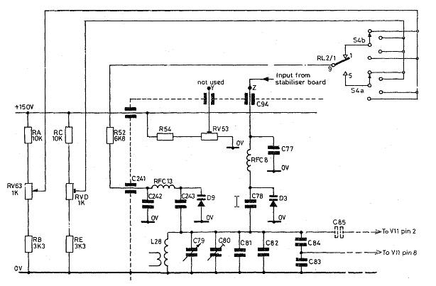
Fig. 4
RVD = 1K linear,RA, RC = 10K RB, RE = 3K3
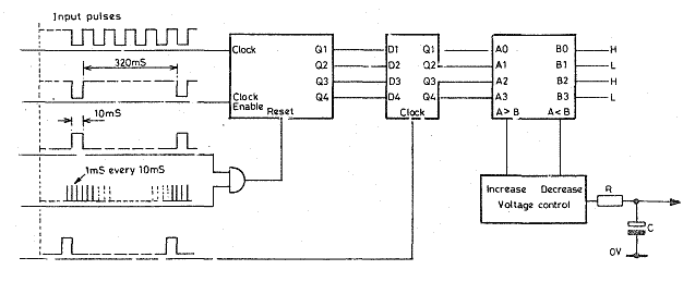
Fig.1.
In this case however, as this signal is connected to the clock enable input (as distinct from the clock inhibit input), the count will be for 320mS, followed by a lOmS inhibit period. As the count is operational for approximately i/3-second, the output from the counter will consist of the four least significant bits representing the frequency in 3 Hz steps, during the lOmS inhibit period the count is applied to the latch, IC15, and the counter is subsequently reset in anticipation of the next count period. The output of the latch is applied to the 'A' input of IC16, a 4-bit magnitude comparator; the 'B' input is set to denary 5 (0101 in binary).
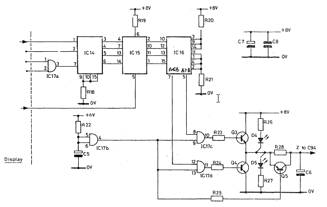
Fig.2.
Two out of the three outputs from the comparator are used, A>B which will go high when the magnitude of input 'A' is from 6 to 9 and A<B, which will go high when the magnitude of 'A' is less than that of 'B', i.e. from 0 to 4. These outputs are fed to the voltage control unit, which applies a voltage (v;a the high resistance resistor, R) to the capacitor С and the varicap diode within the VFO tank circuit. The voltage control unit will increase the voltage across С when A>B, maintain a constant voltage when A = В and decrease the voltage on the capacitor when A<B. The rate of change of voltage is controlled by the values of R and С and the time constant was found to be fairly critical in the author's unit for smooth operation of the stabiliser, although a large range of values was tried and gave satisfactory results.
If either R or С are of too small a value, a noticeable 'warbling tone' is produced due to rapid changes in the value of voltage as the stabiliser overshoots its locking point. Conversely, if R and С are of too large a value, the stabiliser will not be able to cope with the large frequency drifts occurring soon after turn-on and lock will be lost. The locking point exists when the condition A = В = 5 occurs within the magnitude comparator, at which point a constant voltage will be present on the varicap diode. The locking points occur at approximately 33 Hz steps, once the tuning is set onto a specific frequency, and the unit will lock to the nearest step and remain there until the tuning is again adjusted. Assume that the VFO drifts slightly high of the locking point (;'. e. by more than 3 Hz): as the VFO frequency rises, the output from the subtractive mixer will fall, in turn causing the magnitude of 'A' to fall. A<B will go high, decreasing the voltage on the varicap, increasing the effective capacitance in the tank circuit and lowering the VFO frequency. This action will take place until the condition A = В = 5 is attained, upon which the voltage'once again returns to a constant value. Using this method of locking, drifts in either direction can be catered for, enabling even the most stubborn of oscillators to be 'tamed' easily.
Fig. 2 details the schematic diagram of the unit. The operation follows that'of the block diagram but with one important additional facility. For the effective operation of the unit it is essential that the capacitor С (С6 in Fig. 2) is charged to its steady state value (in the case of this unit, 4 volts) before any attempt at stabilisation is made; failure to do this will result in the capacitorbeing only partially charged on the formation of the first locking point, and if a positive VFO drift occurs (causing A<B) then the amount by which the capacitor can discharge will be severely limited — in turn limiting the amount of stabilisation possible.
Conclusion
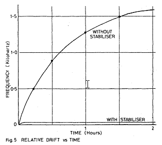
The improvement in stabilisation is best illustrated with the aid of Fig. 5, graphically showing drift of the VFO with and without stabilisation, relative to the frequency at transceiver turn-on (valves having warmed up of course!). In both cases the drift was measured at an initial frequency of 2.600 MHz, at an ambient temperature of 15°C, ensuring similar heating cycles. Operation of the transceiver is made much simpler, frequency stability being in the order of that given by most present day synthesised transceivers — admittedly without some of the facilities of the modern 'Far East wonders', but then again at a fraction of the cost.
 Undoubtedly, within a few weeks the lid will be off the rig again as yet another
mod. is performed — in fact the author has already some ideas on improving sensitivity on the higher frequency
bands; well, fingers crossed. . . .
Undoubtedly, within a few weeks the lid will be off the rig again as yet another
mod. is performed — in fact the author has already some ideas on improving sensitivity on the higher frequency
bands; well, fingers crossed. . . .
It is also pointless attempting to stabilise the VFO frequency immediately following turn-on, as drift during the first minute or so is inevitable in any valve equipment. Both the initial charging circuit and stabilisation inhibit circuits are controlled by the one-shot monostable consisting of R22, C5 and IC176. When the supply voltage is connected, C5 charges via R22, causing a low output from the gate IC17& until a threshold voltage is reached, upon which the output goes high. The delay produced by the circuit is in the region of two minutes, after which control signals are extended via IC17c-d to the voltage controller transistors Q3 andQ4; ifneitherQS or Q4 are conducting, a voltage of 4V will be present at point 'M' and both LEDs will glow dimly. If Q3 is conducting, a voltage of approximately 8V will be present at 'M' and D5 will glow brightly, indicating a charge condition. Similarly, when Q4 conducts, a voltage of approximately 0V will be present at 'M' and D4 will be illuminated, indicating the discharge (or A<B) condition. From the table of values, it can be seen that R28 (shown as R in Fig. 1) and C6 (C in Fig. 1) are of comparatively large value. To effectively charge C6 to the 4V value was found to take around 10 minutes; obviously this time interval is excessive. The addition of R25 and Q5 will effectively short-circuit R28 for the duration that the output of 1С17Й is at logic 0, becoming a virtual infinite resistance as soon as the output flips to the '!' state. In this way, very effective initial turn on charging occurs, whilst maintaining a sufficiently Ugh R, С time constant.
Modifications
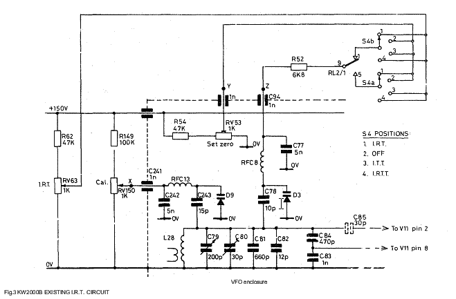
Figs. 3 and 4 detail the relevant parts of the VFO circuitry before and after modification, points 'X' (connected to purple wire), 'Y' (blue wire) and 'Z' (yellow wire) being connections to feedthrough capacitors on the bottom of the VFO enclosure. Note that the roles of the varicap diode branches are in fact reversed; that is, the one which was used for the IRT circuitry before modification is now used for the stabiliser, the diode branch previously used in the calibrate circuitry now being used for the IRT. The addition of the four resistors, RA to RE, will reduce the effective spread of the IRT control from ±6 kHz (which the author found very awkward — requiring 'safe cracker' fingers to net precisely on frequency) to a less daunting ±600 Hz. The complete stabiliser should be placed in a screened box (in the same box as the display unit if possible), with D4 and D5 mounted in the lid of the box so that operation of the stabliser may be readily checked.
![]()
